The acquisition of a surface X-ray diffractometer for the SPEC laboratory at CEA
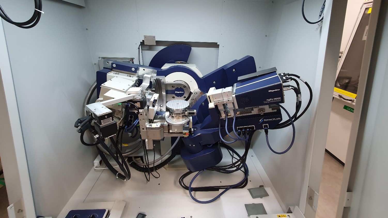
In December 2023, the SPEC laboratory at CEA Saclay acquired a reconditioned X-ray diffractometer, a demonstration instrument supplied by the manufacturer RIGAKU. This new instrument will be used to measure the roughness of interfaces and surfaces, as well as the crystalline quality of thin films fabricated by epitaxy, whether using molecular jets or pulsed lasers, for systems relevant to the field of spintronics. The instrument has been fully operational since 15 March 2024
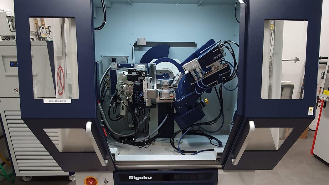
Surface X-ray diffractometer
A commercial agreement has been reached with Rigaku for a SmartLab XE with a 9 kW rotating copper anode. To date, this is the most complete geometry (in the laboratory) and the most powerful anode (the anode is the electrode where oxidation occurs in an electrical or electrochemical device) commercially available for a diffractometer of this type. In addition, the diffractometer is equipped with a Hypix 2D detector, a Ge(220)x2 monochromator and various optical elements for conditioning the beam or modulating the resolution in reciprocal space. This instrument will be very useful for the SPINMAT Transverse Project.
What are the objectives?
Devices based on spin electronics rely heavily on thin films (below a few tens of nanometres). When all the atoms are arranged in a perfectly well-defined and ordered network, we speak of single-crystal layers. These particular arrangements can give rise to anisotropies that can be exploited in the transport of spin currents, but also make it possible to exploit the stresses that the layers can exert on each other at sufficiently small thicknesses.
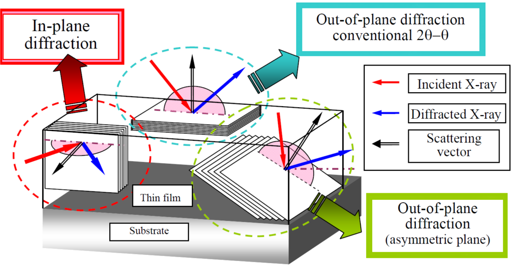
The intensity of X-rays diffracted by a sample depends on the density and quantity of material. In the case of thin layers, a drop in intensity of several orders of magnitude is to be expected (6 orders of magnitude for a surface compared with a volumetric sample). This drop in intensity can be compensated for by using a source that supplies a higher number of photons and a grazing incidence geometry that is better suited to this type of study object. However, this requires a more complex goniometer with at least 5 circles, which is the case with the SmartLab.
His functioning :
